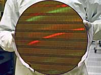
Chips push through nano-barrier
Source: news.bbc.co.uk
 New materials have had to be developed to shrink the transistors
The next milestone in the relentless pursuit of smaller, higher performance microchips has been unveiled.
Chip-maker Intel has announced that it will start manufacturing processors using transistors just 45 nanometres (billionths of a metre) wide.
Shrinking the basic building blocks of microchips will make them faster and more efficient.
Computer giant IBM has also signalled its intention to start production of chips using the tiny components.
"Big Blue", which developed the transistor technology with partners Toshiba, Sony and AMD, intends to incorporate them into its chips in 2008.
Intel said it would start commercial fabrication of processors at three factories later this year.
Critical leaks
The development means the fundamental "law" that underpins the development of all microchips, known as Moore's Law, remains intact.
The proposition, articulated by Intel co-founder Gordon Moore in 1965, states that the number of transistors on a chip could double every 24 months.
The new Intel processors, codenamed Penryn, will pack more than four hundred million transistors into a chip half the size of a postage stamp.
Like current processors, they will come in dual-core and quad-core versions, meaning they will have two or four separate processors on each chip. The company has not said how fast the new devices will run.
The production of 45nm technology has been the goal of chip manufacturers ever since they conquered 65nm transistors.
A transistor is a basic electronic switch. Every chip needs a certain number of them, and the more there are and the faster they can switch, the more calculations chips can do.
For more than 45 years, chip manufacturers have managed to keep up with Moore's Law, shrinking transistor size and packing more and more of them on to chips.
However, past the 65nm barrier the silicon used to manufacture critical elements of the switches known as gate dielectrics no longer performs as it does at larger scales.
As a result, currents passing through the transistors leak and reduce the effectiveness of the chip.
To prevent this, researchers have had to develop new materials to contain the current at such small scales. The class of silicon substitutes are known as high-k metals.
Same 'tools'
Their development and integration into working components was described by Gordon Moore as "the biggest change in transistor technology" since the late 1960s.
The first working chips to incorporate 45nm devices were demonstrated last year by Intel, but they have never been incorporated into commercial products.
Dr Tze-chiang Chen, vice president of science and technology at IBM Research, said: "Until now, the chip industry was facing a major roadblock in terms of how far we could push current technology.
"After more than 10 years of effort, we now have a way forward."
The exact recipes for the different high-k metals used by Intel and IBM have not been disclosed, but importantly both firms have said that they could be incorporated into current production technology with minimal effort.
Article from: http://news.bbc.co.uk/1/hi/technology/6299147.stm


